The joint efforts of UNIPR, UNIMORE and IMEM led to fabrication of innovative photodiodes based on n-type epitaxial Ga2O3 and overgrown inorganic or organic p-type layers.
Different examples of photodiodes are provided in the figures below:
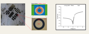
Fig. 1: Ga2O3-based planar PN junction diode and I-V characteristics in dark
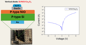
Fig. 2: Ga2O3-based vertical PN junction diode and I-V characteristics
Performance of the self-powered photodiodes
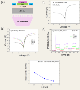
The following figures reports typical responsivity and response time of a κ-Ga2O3 /NiO vertical photodiode illuminated from the rear across the transparent sapphire substrate. This configuration may be used as a broadband detector, in which the UV-C spectrum can excite the GaO layer while the photons of lower energy will excite the NiO film. This device can operate at 0 bias (self-powered).
Fig. 3: Structure and performance of planar κ-Ga2O3 / NiO photodiode
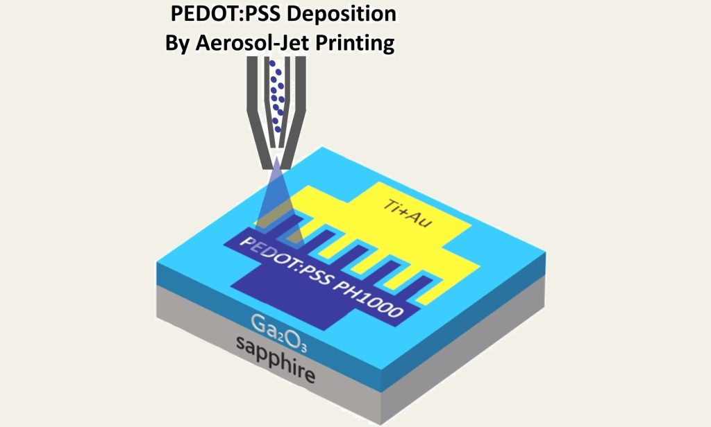
Photodiodes based on a planar hybrid heterojunction between Ga2O3 and an organic semiconductor have been fabricated.
Fig: 4: Sketch of the completed hybrid Ga2O3/PEDOT:PSS diodes with a custom-made interdigitated shape of the contacts.
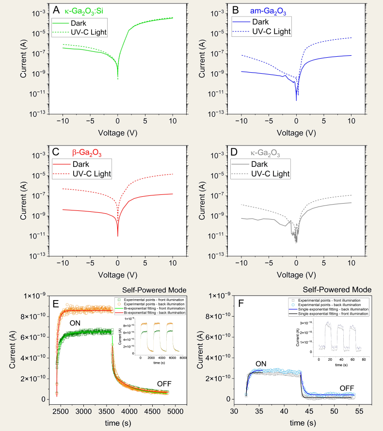
Fig. 5: I-V curves of the devices fabricated using (A) silicon-doped κ-Ga2O3, (B) am-Ga2O3, (C) β-Ga2O3, (D) κ-Ga2O3. Fit of the transient photocurrent normalized by the incident luminous power (E) in the case of the device based on β-Ga2O3 and (F) for the am-Ga2O3 based device. The insets show the complete measurement data with repeated cycles of exposition to the UV-C light source (∼1 μW/cm2 for λ = 250 nm).
Simulation of device operation and properties
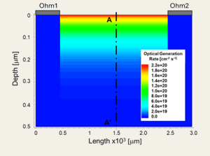
Modelling and simulation are important activities in USEGAO. The following figure provides an example of simulation applied to a photoresistor based on κ-Ga2O3.
Fig. 6: 2D contour plot of the optical generation rate within the simulated Ga2O3 photoresistor. Ohm1 and Ohm2 are the two ohmic contacts. A-A’ is the cutline along which the distributions of photocarriers were calculated (see Fig. 5)
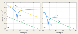
Fig. 7: 1D plot along the A-A’ line of the following quantities: (yellow line) hole trapped charge density, NDON+, (green line) hole density, p, (red line) electron density, n, and (blue line) net space-charge density, ρ=NDON+-n+p. Deep donor density is assumed to be NDON=1016 cm-3 and 0 in (a) and (b), respectively
This type of simulation was useful in order to better understand and quantify the photogain phenomena in GaO-based photoresistors.